PCB Design Tips And Challenges: Master Your Layout Skills!
When it comes to creating efficient and reliable electronic devices, mastering PCB (Printed Circuit Board) design is crucial for engineers and hobbyists alike. The layout of your PCB can significantly impact the performance, reliability, and manufacturability of your final product. However, navigating the complexities of PCB design can present a myriad of challenges, from managing signal integrity to optimizing component placement. In this blog post, we'll explore essential tips and common pitfalls in PCB design, equipping you with the skills to enhance your layout and overcome obstacles like a pro. Whether you're a seasoned designer or just starting out, these insights will help you elevate your PCB projects to the next level!
Pcb Design Tips For Beginners
When diving into the world of PCB design, beginners can significantly enhance their skills by following some essential tips. First and foremost, it's crucial to familiarize yourself with the design software you're using; take advantage of tutorials and online resources to get comfortable with the tools at your disposal. Start with a clear schematic that outlines your circuit's functionality, as this will serve as the backbone of your layout. Pay attention to component placement, ensuring that related components are positioned close together to minimize trace lengths and reduce noise. Additionally, don't overlook the importance of grounding; a solid ground plane can help prevent interference and improve overall performance. Finally, always double-check your work with design rule checks (DRCs) to catch any potential errors before moving to fabrication. By implementing these tips, you'll be well on your way to mastering the art of PCB layout design!
 design.udlvirtual.edu.pe
 5 Typical Pcb Design Challenges With Solutions
When diving into PCB design, engineers often face several common challenges that can impact the functionality and manufacturability of their boards. One typical issue is managing signal integrity, which can be addressed by carefully routing traces and using proper termination techniques. Another challenge is thermal management; incorporating thermal vias and heat sinks can help dissipate heat effectively. Component placement can also be tricky, but using design software that offers 3D visualization can aid in optimizing layout. Additionally, ensuring manufacturability is crucial; collaborating with your PCB manufacturer early in the design process can prevent costly errors. Lastly, maintaining a balance between size and performance can be tackled by utilizing smaller components and advanced layout techniques, ensuring your design meets both space and functionality requirements. By understanding these challenges and their solutions, you can enhance your PCB design skills and create more efficient layouts.
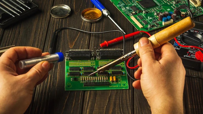
 www.protoexpress.com
 Pcb Design Tips And Challenges
When diving into the world of PCB design, it's essential to understand both the tips that can enhance your layout skills and the challenges you may encounter along the way. One key tip is to prioritize component placement strategically; ensuring that high-frequency components are positioned close together can reduce signal interference and improve performance. Additionally, maintaining a clear ground plane helps minimize noise and enhances signal integrity. However, designers often face challenges such as managing thermal issues and ensuring manufacturability. Balancing trace width and spacing while adhering to design rules can be daunting, especially as complexity increases. By honing your skills and being aware of these hurdles, you can create efficient and reliable PCB layouts that stand the test of time.
 eepower.com
 5 Tips For Better Pcb Design
When it comes to mastering your PCB design skills, implementing a few key strategies can significantly enhance your layout process. First, always prioritize a clear and organized schematic; this foundation will streamline your design and minimize errors. Second, pay close attention to component placement—strategically positioning parts can reduce trace lengths and improve signal integrity. Third, utilize ground planes effectively to minimize electromagnetic interference and enhance performance. Fourth, ensure proper trace width calculations to handle current loads without overheating. Finally, don't underestimate the power of thorough testing and simulation; validating your design before fabrication can save you time and resources in the long run. By following these tips, you'll be well on your way to creating efficient and reliable PCB layouts.
 www.shoutmecrunch.com
 Designing A Flex Pcb Prototype: Pcb Design Tips And Considerations
When designing a flex PCB prototype, there are several key tips and considerations to keep in mind to ensure a successful layout. First, it's crucial to understand the unique characteristics of flexible circuits, such as their bendability and space-saving advantages. Prioritize the placement of components to minimize stress on the PCB during flexing; avoid placing components at the bends and consider the flex direction early in the design process. Additionally, use appropriate materials that can withstand repeated flexing without degrading. Pay attention to trace width and spacing, as thinner traces can be more susceptible to damage. Lastly, always prototype and test your design under real-world conditions to identify potential issues before final production. By following these guidelines, you can enhance the reliability and performance of your flex PCB prototype while mastering the complexities of PCB design.
 in.pinterest.com
 Other Wiring Gallery

www.protoexpress.com
7 Pcb Design Tips By Rick Hartley

hackaday.com
Aesthetic Pcb Design Tips For Improved Functionality

5bestthings.com
Pcb Design Tips Every Engineer And Hobbyist Should Know

just4programmersuk.blogspot.com
Top Tips For Pcb Design Layout

www.raypcb.com
Tips And Tricks To Build Efficient 433mhz Pcb Antenna Design

www.raypcb.com
What Is High Density Pcb?

camptechii.com
18 Pcb Layout Tips For Improving Your Pcb Design And Reducing
