Working with Mechanical Layers in Altium Designer 24: Expert Tips! Working with mechanical layers
Designing electronic circuits and printed circuit boards (PCBs) demands precision, efficiency, and a keen understanding of various software tools. Among these tools, Altium Designer stands out as a comprehensive solution, offering a wide array of features to streamline the design process, from schematic capture to PCB layout and manufacturing documentation. This document presents some insights into utilizing Altium Designer, covering aspects like layer management and custom design approaches.
Altium Designer 17: Layer Management and Camtastic Integration

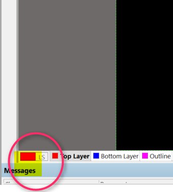
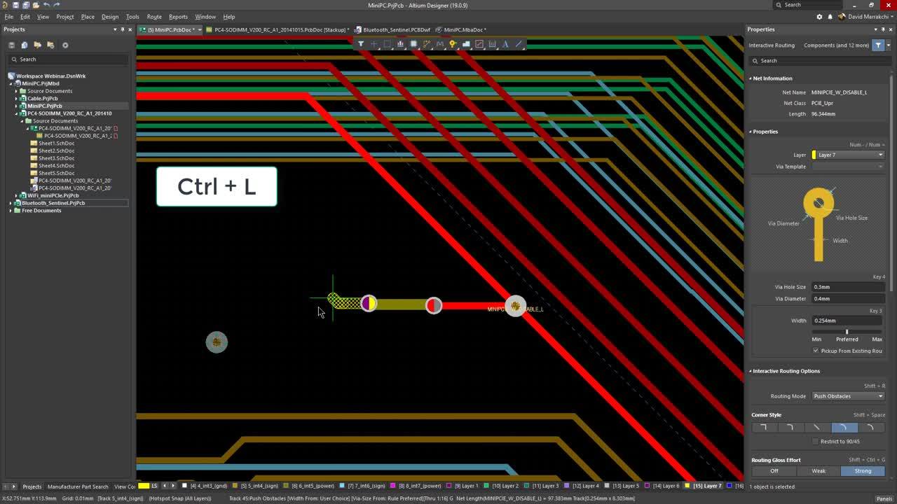
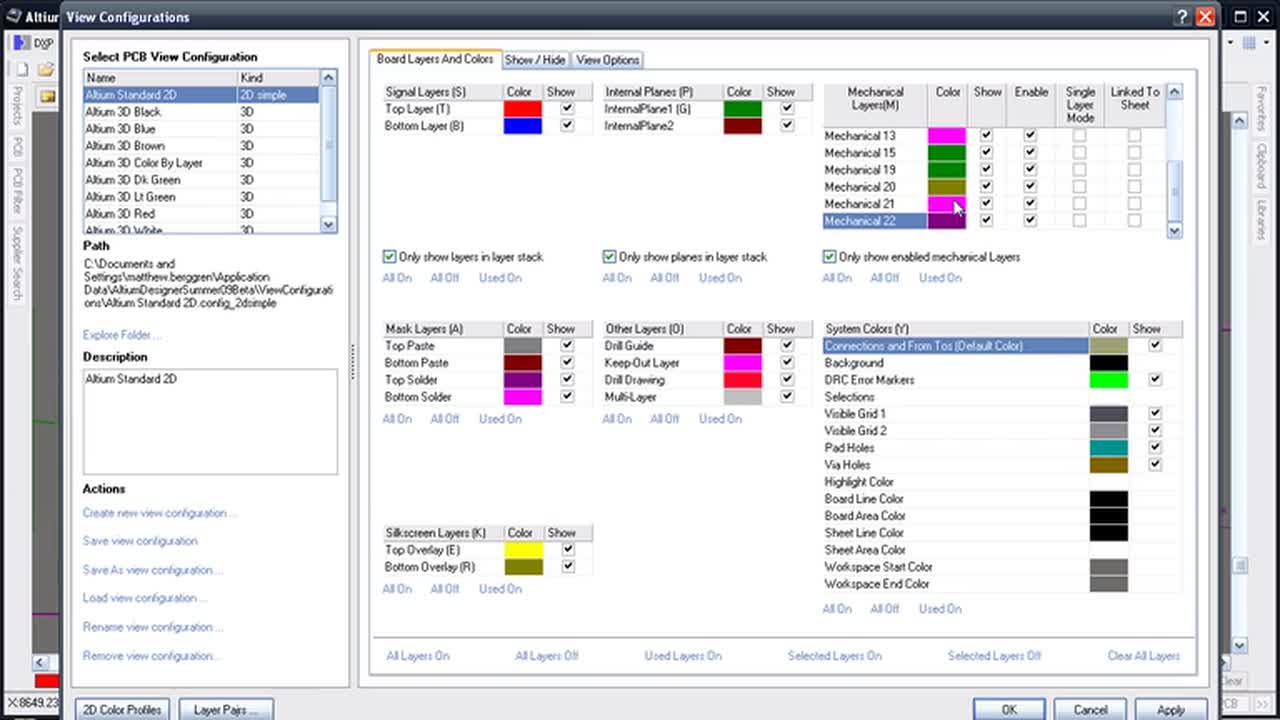
Altium Designer 17 introduced enhancements to its layer management capabilities, particularly within the Camtastic environment. Camtastic, Altium's CAM editor, is crucial for preparing designs for manufacturing. Understanding how to effectively switch and manipulate layers in Camtastic is essential for ensuring the accuracy and manufacturability of PCBs. A crucial aspect of PCB design is the ability to isolate and modify specific layers without affecting others. This is particularly relevant when dealing with complex multi-layer designs. Camtastic allows users to selectively enable or disable layers, making it easier to identify potential issues, verify clearances, and optimize the design for manufacturing processes such as etching and drilling. The ability to accurately review and modify individual layers within Camtastic is vital for resolving design rule check (DRC) violations and ensuring that the final product meets all required specifications.
The ability to manipulate layers extends beyond simple visibility control. Camtastic provides tools for editing layer data, such as modifying copper traces, adjusting drill hole sizes, and adding or removing elements. This level of control is invaluable when addressing specific manufacturing constraints or making last-minute design changes. For instance, a designer might need to adjust a trace width on a particular layer to accommodate a tighter impedance requirement or increase the clearance between vias to improve signal integrity. By leveraging Camtastic's layer manipulation capabilities, designers can make these adjustments directly within the manufacturing environment, reducing the risk of errors and improving the overall efficiency of the design process.
Custom Design Approaches: Mechanical and Keep-Out Layers

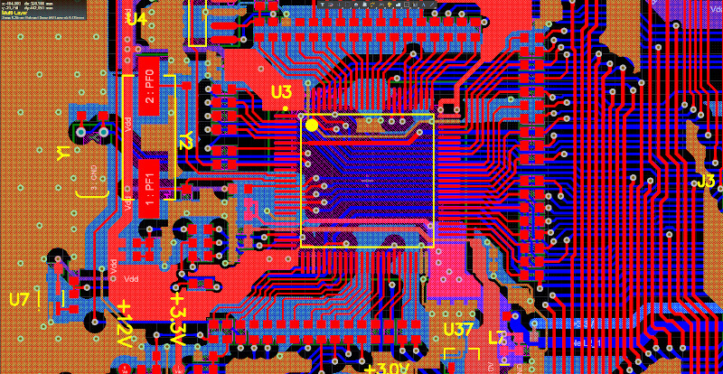
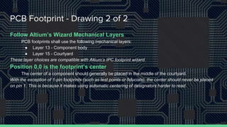
Beyond the standard signal and power layers, Altium Designer offers flexibility through the use of mechanical layers and keep-out layers. These layers play crucial roles in defining the physical characteristics of the PCB and ensuring proper component placement. Mechanical layers are used to convey information about the board's physical dimensions, mounting holes, and other mechanical features. This information is essential for both manufacturing and assembly processes. For example, a mechanical layer might specify the location of mounting holes for securing the PCB within an enclosure or define the board's outline for routing and panelization. Properly defining mechanical layers ensures that the PCB fits correctly within its intended environment and that all necessary mounting hardware can be accommodated. These layers also help in communicating critical dimensions to the fabrication house, reducing the chance of errors during the manufacturing process.
Keep-out layers, on the other hand, are used to restrict component placement and routing in specific areas of the PCB. This is particularly useful for preventing interference from heat-sensitive components, high-voltage circuits, or RF signals. By defining keep-out areas, designers can ensure that critical components are isolated and that routing is restricted to areas where it will not compromise the board's performance or reliability. For example, a keep-out layer might be used to prevent components from being placed too close to the edge of the board, where they could be vulnerable to damage during handling. Alternatively, a keep-out layer might be used to isolate sensitive analog circuitry from noisy digital components, preventing unwanted signal interference. The strategic use of keep-out layers can significantly improve the performance and robustness of the PCB design, especially in high-density or high-performance applications. Effective use of these layers can improve manufacturability and prevent issues during the assembly process.
If you are searching about How do you Add/Remove design layers - element14 Community you've visit to the right page. We have 25 Images about How do you Add/Remove design layers - element14 Community like Working with Mechanical Layers | Altium Designer 25 and 24 Technical, Working with Mechanical Layers | Altium Designer 25 Technical Documentation and also Altium Designer 25 is Here | Altium. Here you go:
How Do You Add/Remove Design Layers - Element14 Community
 community.element14.com
 Altium Designer 25 Is Here | Altium
 www.altium.com
 Tips For Altium Designer Beginners To Solve Common PCB Layout Problems
 www.pcbaaa.com
 Flex And Rigid-Flex PCB Design Guidelines And Assembly In Altium
 resources.altium.com
 layer altium flex pcb rigid stackup circuit guidebook regions organizing ensure
How To Switch Layers During Routing In Altium Designer 19
 resources.altium.com
 Altium Designer Electronic Design Services | Develer
 www.develer.com
 Working With Mechanical Layers | Altium Designer 25 Technical Documentation
 www.altium.com
 Unlimited Mechanical Layers In Altium Designer - YouTube
 www.youtube.com
 altium mechanical layers
6-Layer PCB Stackup Design Guidelines | Zach Peterson | Industry Expert
 resources.altium.com
 Working With Mechanical Layers | Altium Designer 25 Technical Documentation
 www.altium.com
 Working With Mechanical Layers | Altium Designer 25 Technical Documentation
 www.altium.com
 Altium Component Library Standards | PPT
 www.slideshare.net
 Additional Mechanical Layers - Features:ADSCvid | Altium
 resources.altium.com
 Managing Layers | Altium Designer 25 Technical Documentation
 www.altium.com
 Output Mechanical Drawings In Altium Designer 16 - Loverlena
 loverlena.weebly.com
 [Altium] Using Mechanical Layers And Keep Out Layers In Custom
www.reddit.com altium
Working With Mechanical Layers | Altium Designer 25 Technical Documentation
 www.altium.com
 Altium Help - Adding Mechanical Layers : R/PrintedCircuitBoard
 www.reddit.com
 Output Mechanical Drawings In Altium Designer 16 - Taiasummit
 taiasummit.weebly.com
 Altium Help - Adding Mechanical Layers : R/PrintedCircuitBoard
 www.reddit.com
 Working With Mechanical Layers | Altium Designer 25 Technical Documentation
 www.altium.com
 Altium Change Layer Color
 userengineenology.z14.web.core.windows.net
 Altium Designer 17 Camtastic Switch Layers - Kickluda
kickluda.weebly.com Working With Mechanical Layers | Altium Designer 25 And 24 Technical
 www.altium.com
 Altium Designer Quick-Start Tutorial | Phil's Lab | Industry Expert
 resources.altium.com
 How to switch layers during routing in altium designer 19. How do you add/remove design layers. Additional mechanical layers